555-Driven LED Bar Graph
Two chips, eight LEDs, and one clock signal deciding exactly when each light joins the bar — the moment you power this circuit up, a single LED appears, then a second, then a third, until all eight are lit. Press a button and the whole bar drops back to dark, ready to fill again.
The capstone build, builder!
 This is the payoff lab for everything Chapter 14 and Chapter 15 taught you. You already know how to wire a 555 clock (Lab 45) and how a 74HC595 shifts bits into eight outputs. Today those two skills become one circuit — the 555 becomes the shift register's heartbeat, with no code and no microcontroller anywhere in sight. Let's light it up!
What You'll Learn
By the end of this lab you will be able to:
- Build a two-chip circuit where a 555 astable clock drives a 74HC595 shift register
- Wire SER, OE′, and SRCLR′ to their correct fixed logic levels and explain what each connection accomplishes
- Predict and observe why bridging SRCLK and RCLK together makes every clock pulse both shift a bit in and latch it out immediately
- Calculate the 555's clock frequency for this lab's R1, R2, and C1 values
- Diagnose the wiring mistakes specific to a two-chip build, from a backward IC to an unbridged clock pin
Before You Start
| Time | 60-75 minutes — the longest, most parts-heavy build in this book |
| Difficulty | Intermediate — a two-chip capstone build |
| You should already know | Chapter 14: The 555 Timer Chip and Chapter 15: Shift Registers and IC Handling, including how to straddle a DIP chip across the centre channel |
| Strongly recommended first | Lab 45: 555 Timer LED Blinker — this lab reuses that exact 555 clock circuit, just aimed at a different pin |
What You'll Need
Everything here is in the $50 kit.
| Qty | Part | Value or marking | How to spot it |
|---|---|---|---|
| 1 | Breadboard | half-size, 30 columns | the white plastic board with rows of holes |
| 1 | 555 timer IC | NE555, 8-pin DIP | small black chip; a notch or dot at one end marks pin 1 |
| 1 | 74HC595 shift register IC | 74HC595, 16-pin DIP | longer black chip, same notch-marks-pin-1 rule |
| 1 | Resistor | 1 kΩ (R1) | tan body, bands brown-black-red, then gold |
| 1 | Resistor | 13 kΩ (R2) | tan body, bands brown-orange-orange, then gold |
| 1 | Resistor | 10 kΩ (R9) | tan body, bands brown-black-orange, then gold |
| 8 | Resistor | 330 Ω | tan body, bands orange-orange-brown, then gold |
| 1 | Capacitor | 10 µF electrolytic | small cylinder; one lead marked +, a stripe marks the other side |
| 8 | LED | any color, 5 mm | one leg longer than the other |
| 1 | Push button | momentary, 4-leg tactile | small square button that only connects while pressed |
| ~20 | Jumper wires | assorted colors | |
| 1 | Power supply | 5 V USB, or a 3×AA battery pack | any phone charger with a USB-A male-to-male cable |
Only have 4-6 matching LEDs?
 That's completely fine — wire fewer Q outputs (Q0, Q1, Q2, Q3 is a great starting set) and leave the rest disconnected. The pattern scales to however many outputs you wire: the bar just fills up to your LED count instead of eight. Nothing else about the circuit changes.
R9 is not part of the "official" 74HC595 pinout — it is this lab's own safety addition. Chapter 15 tells you SRCLR′ (pin 10) is normally held high; the simplest way to do that is a resistor to +5 V rather than a bare wire, so that pressing the reset button never connects +5 V straight to ground. You'll see exactly why in How It Works.
Safety First
At 5 volts, none of this can shock you. Two habits matter here more than in any earlier lab, because this build has two chips and a lot of wiring:
- Wire everything first, plug in power last — no exceptions. With this many connections, a live rewire is the easiest way to create a short circuit by accident.
- Check both notches before you wire a single pin. Both the 555 and the 74HC595 have a notch (or dot) marking pin 1. A chip inserted backward gets its power and ground pins swapped, which can damage it the instant power is applied.
- Ground yourself before handling the 74HC595. It's a CMOS chip, which makes it more sensitive to static electricity than the 555. Touch a grounded metal object for a second before you pick it up — a bare table leg, an unpainted radiator, or a plugged-in computer's case all work.
- Straddle the centre channel correctly on both chips. Off by even one row and half the chip's pins land in the wrong net, with no visible sign anything is wrong.
Try It in the Simulator
Before wiring anything, watch this exact circuit's behavior in Chapter 15's shift-register simulator.
Two controls to try, in this order:
- Check the "555-driven clock" box. The manual "Clock Pulse" button disappears and the register starts advancing on its own — that automatic pulsing is exactly what your real 555 is about to do to SRCLK.
- Watch the LEDs fill up, then click "Reset (clear)." The bar drops to all zero and starts filling again. That button is the sim-side preview of the physical push button you're about to wire.
That fill-then-clear rhythm is the entire lab. Everything below is about building the real thing.
The Circuit Diagram
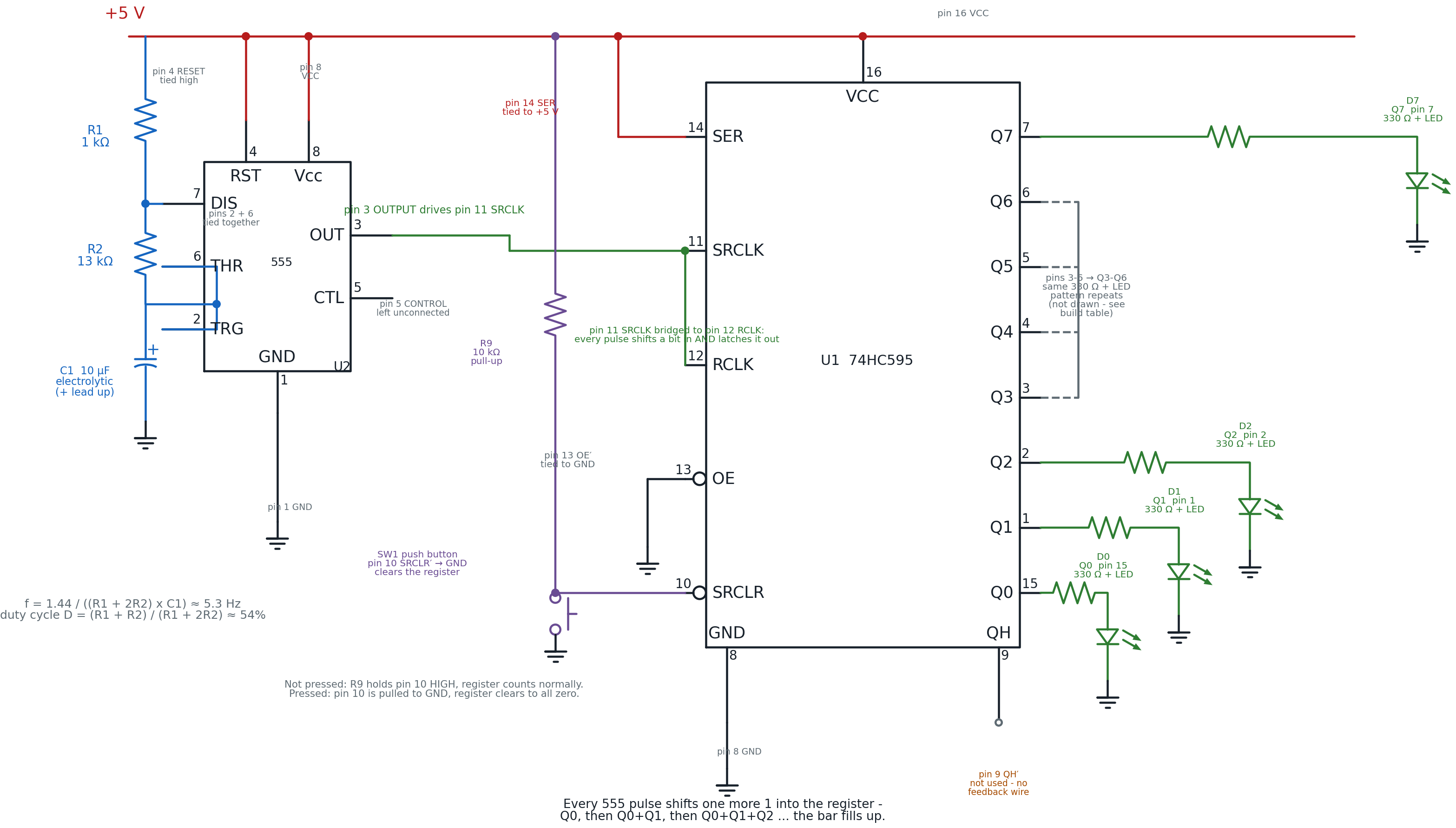
Trace the clock path: +5 V feeds the 555's VCC (pin 8) and RESET (pin 4). R1, R2, and C1 set how fast pin 3 (OUTPUT) swings high and low. That output goes to exactly one place — the 74HC595's SRCLK (pin 11), which is bridged straight across to RCLK (pin 12).
One wire, two jobs
 Normally SRCLK and RCLK are two separate control lines — one shifts a bit in, the other reveals it on the LEDs. Bridging them together means every single 555 pulse does both jobs at once. That's the trick that makes this circuit work with no extra wiring and no code.
The Breadboard Layout
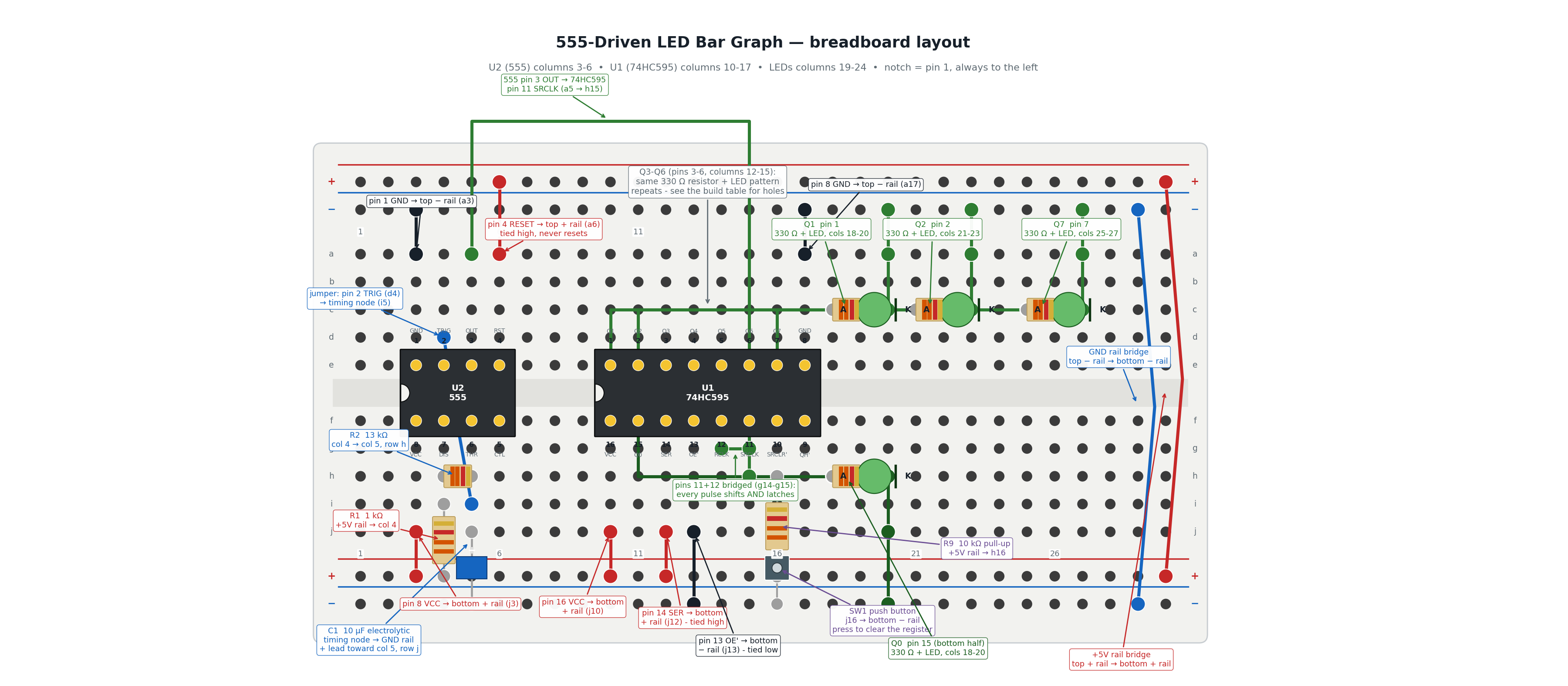
This is the widest board in the book, and it uses both the top and bottom power rails — reach for whichever rail is physically closer to the pin you're wiring.
| In the schematic | On the breadboard |
|---|---|
| 555, pins 1-4 | Row e, columns 3-6 (notch at column 3) |
| 555, pins 8-5 | Row f, columns 3-6, mirrored |
| R1 (1 kΩ) | Bottom + rail → i4 (pin 7's own column) |
| R2 (13 kΩ) | h4 → h5 (pin 7's column to pin 6's column) |
| Jumper: pin 2 → timing node | d4 → i5 |
| C1 (10 µF, + up) | j5 → bottom − rail |
| 74HC595, pins 1-8 | Row e, columns 10-17 (notch at column 10) |
| 74HC595, pins 16-9 | Row f, columns 10-17, mirrored |
| 555 pin 3 → SRCLK | a5 → h15, routed above the top rail |
| SRCLK ↔ RCLK bridge | g14 → g15 |
| R9 (10 kΩ pull-up) | Bottom + rail → h16 |
| SW1 (push button) | j16 → bottom − rail |
| Q0 branch (bottom half), pin 15 | f11 → jumper → h18 → resistor → h19 → LED → h20 → jumper → bottom − rail |
| Q1 branch, pin 1 | e10 → jumper → c18 → resistor → c19 → LED → c20 → jumper → top − rail |
| Q2 branch, pin 2 | e11 → jumper → c21 → resistor → c22 → LED → c23 → jumper → top − rail |
| Q7 branch, pin 7 | e16 → jumper → c25 → resistor → c26 → LED → c27 → jumper → top − rail |
| Rail bridges | Top − rail ↔ bottom − rail at column 29; top + rail ↔ bottom + rail at column 30 |
Each LED branch is four parts in a row, not one: a jumper carries the pin's signal over to a fresh column, a resistor bridges from there to the LED's anode column, the LED itself bridges to the cathode column, and a final jumper drops the cathode to a ground rail. It looks like one long chain in the table above, but every arrow is a separate physical part.
Two things worth noticing before you build. First, row e and row f at the same column number are not connected — that gap is the centre channel. A pin on the top half (like the 555's TRIGGER) needs its own jumper to reach a pin on the bottom half (like THRESHOLD), even though the schematic just draws one line between them. Second, the rail bridges at columns 29 and 30 are not optional decoration. Without them, the top rails and bottom rails are two separate, disconnected power buses, and half your circuit goes dark.
Build It
Work down this list in order. Both chips go in — and get checked — before a single wire is connected.
- Leave the power unplugged. Nothing touches the supply until the very last step.
- Touch something grounded before you open the 74HC595's packaging — a static discharge is invisible and can damage a CMOS chip silently.
- Insert the 555 straddling the centre channel, notch facing column 3. Pins 1-4 land in row e; pins 8-5 land in row f.
- Insert the 74HC595 straddling the centre channel, notch facing column 10. Pins 1-8 land in row e; pins 16-9 land in row f.
Stop. Verify both notches before you wire anything.
 Look at both chips from above right now. The 555's notch should face column 3; the 74HC595's notch should face column 10. A chip inserted backward swaps its power and ground pins with signal pins — on the CMOS 74HC595 especially, that can damage the chip the instant power reaches it. Checking now costs ten seconds. Fixing a cooked chip costs a trip back to the parts bin.
- Run a jumper from the top − rail down to the bottom − rail at column 29 (the GND rail bridge).
- Run a jumper from the top + rail down to the bottom + rail at column 30 (the +5 V rail bridge).
- Run a jumper from the top − rail to a3 (555 pin 1, GND).
- Run a jumper from the top + rail to a6 (555 pin 4, RESET — tied high so it never interrupts the clock).
- Run a jumper from the bottom + rail to j3 (555 pin 8, VCC).
- Bridge the 1 kΩ resistor (R1) from the bottom + rail to i4.
- Bridge the 13 kΩ resistor (R2) from h4 to h5.
- Run a jumper from d4 (pin 2, TRIGGER) to i5 (the timing node).
- Place C1 (10 µF electrolytic): + lead in j5, − lead in the bottom − rail.
- Run a jumper from the top − rail to a17 (74HC595 pin 8, GND).
- Run a jumper from the bottom + rail to j10 (74HC595 pin 16, VCC).
- Run a jumper from the bottom + rail to j12 (pin 14, SER — a logical 1 is now always waiting to shift in).
- Run a jumper from j13 (pin 13, OE′) to the bottom − rail (outputs always enabled).
- Bridge g14 to g15 — this ties pin 12 (RCLK) directly to pin 11 (SRCLK).
- Bridge the 10 kΩ resistor (R9) from the bottom + rail to h16.
- Wire the push button (SW1) from j16 to the bottom − rail.
- Run a jumper from a5 (555 pin 3, OUTPUT) up above the top rail and over to h15 (74HC595 pin 11, SRCLK). This is the wire that turns the shift register's clock over to the 555.
Checkpoint before the LEDs
Pause here and trace it out loud: +rail → R1 → R2 → timing node → pins 2 and 6. Separately: pin 3 → SRCLK, and SRCLK → RCLK. If you had a multimeter, pin 3 and pin 11 should read the exact same voltage right now — they're the same net.
- For Q1 (pin 1, at e10): jumper e10 to c18. Bridge a 330 Ω resistor from c18 to c19. Place the LED's long leg (anode) in c19 and short leg (cathode) in c20. Jumper c20 to the top − rail.
- For Q0 (pin 15, at f11): jumper f11 to h18. Bridge a 330 Ω resistor from h18 to h19. Place the LED's anode in h19 and cathode in h20. Jumper h20 to the bottom − rail.
- For Q2 (pin 2, at e11): jumper e11 to c21. Bridge a 330 Ω resistor from c21 to c22. Place the LED's anode in c22 and cathode in c23. Jumper c23 to the top − rail.
- For Q7 (pin 7, at e16): jumper e16 to c25. Bridge a 330 Ω resistor from c25 to c26. Place the LED's anode in c26 and cathode in c27. Jumper c27 to the top − rail.
- Q3, Q4, Q5, and Q6 use the identical four-part pattern as Q2 — jumper, resistor, LED, jumper to a rail. Their pins live at e12, e13, e14, and e15. Wire as many of these four as you have LEDs and board space for, choosing any free columns to their right — even two or three more makes the fill-up effect more dramatic.
- Checkpoint — before power. Look at every LED. Every anode (long leg) should face its resistor; every cathode (short leg) should face its rail jumper. Confirm SW1 sits between column 16 and the bottom − rail, not anywhere near +5 V.
- Predict first. The instant you apply power, what do you expect to see — all eight LEDs on at once, all eight off, or something else? Write your guess down before you plug in.
- Plug in the 5 V supply. Watch the bar fill up: one LED, then two, then three, on up to however many you wired — then press SW1 and watch it drop back to dark and start again.
You are done when you can watch the LEDs fill up in order, clear them with SW1, and watch them fill again — repeatably, with no wires touched after power-up.
You just ran two chips as one circuit!
 Look at what you built: a clock chip and a shift register, talking to each other through exactly one wire. Together they fill up a bar of light and clear it on command — no code, no computer, just silicon doing arithmetic on a schedule you designed. That's a real two-chip system, and you're the one who wired it. Current's flowing your way!
How It Works
Three design choices make this circuit work, and each one answers a specific question.
Why is SER tied straight to +5 V? SER (pin 14) is the "next bit to shift in" pin. Tying it permanently to +5 V means the answer to "what's the next bit?" is always 1 — a logical 1 is permanently waiting at the door. Every time a clock pulse arrives, that 1 gets shifted in, and everything already inside the register moves one position over.
Why does bridging SRCLK and RCLK make the bar fill up instead of chase? Normally SRCLK (shift) and RCLK (latch/reveal) are separate signals, so a program can shift several bits in privately before revealing the whole pattern at once. This lab skips that separation on purpose. Tying SRCLK and RCLK together means the instant a bit shifts in, it's also latched out to the visible LEDs — shift and reveal happen in the same clock pulse, every time. Combined with SER being permanently 1, each pulse doesn't just move a dot — it adds one more lit LED to everything already lit. Q0 lights first, then Q0 and Q1 together, then Q0, Q1, and Q2 together, and so on until the whole bar is lit. That's a fill-up pattern, not a single moving dot — an important distinction from a true "walking LED" chaser, which needs a feedback wire this lab deliberately leaves out.
Why does R9 exist, and why does pressing SW1 clear the register? SRCLR′ (pin 10) is active-low: pull it to ground and every stored bit resets to zero. R9 holds that pin at +5 V through a resistor rather than a bare wire, so the pin reads a solid HIGH when SW1 is untouched. Press SW1, and it connects pin 10 directly to ground. R9 limits the current to a safe 5 V ÷ 10 kΩ ≈ 0.5 mA instead of creating a dead short across the supply. The register instantly clears, every LED goes dark, and the fill-up starts over on the very next clock pulse.
Finally, the clock rate itself is pure Chapter 14 math — the same astable formula from Lab 45, with different resistor values.
That's about 5.3 clock pulses per second — fast enough that the bar fills up in a little over a second, but slow enough to watch each LED join in.
Where you've seen this before
 A phone charging animation. A signal-strength bar on a router. A loading meter on an old game console. All of them are some version of exactly this: a clock stepping a register that reveals one more segment each time.
When It Doesn't Work
Work down this list in order — check power and orientation before you check anything clever.
| What you see | Likely cause | Fix |
|---|---|---|
| Nothing lights, one chip runs warm | A chip is inserted backward | Unplug power immediately, pull the chip, and reinsert it with the notch at column 3 (555) or column 10 (74HC595) |
| Nothing lights at all | Rail bridges missing | Check the jumpers bridging the top and bottom − rail (column 29) and + rail (column 30) — without them, half the circuit has no power or ground |
| All LEDs stay dark, register never fills | SER not actually tied to +5 V | Recheck the jumper from pin 14 to the bottom + rail — with no 1 waiting to shift in, the register only ever fills with zeros |
| LEDs never change, even though the 555 is clearly oscillating | SRCLK and RCLK are not actually bridged | This is the trickiest failure in this lab: bits are shifting into the chip's hidden stage every pulse — they're just never being revealed. Recheck the g14-g15 jumper. A single manual jumper touch to RCLK would instantly show the pattern that was already there |
| Pressing the button does nothing | SW1 wired to the wrong pin, or wired to OE′ instead of SRCLR′ | SW1 must bridge column 16 (pin 10, SRCLR′) to the − rail — not column 13 (OE′), which only blanks the display without erasing it |
| One LED never lights, the rest do | That LED is backwards | Long leg (anode) toward its resistor, short leg (cathode) toward its rail jumper |
| Bar fills but never clears fully | R9 missing or on the wrong pin | Without R9 pulling SRCLR′ high, the pin can float and behave unpredictably; confirm R9 bridges the bottom + rail to column 16 |
| Everything works but very dimly | A 330 Ω resistor swapped for a much larger value | 330 Ω is correct for these LEDs at 5 V |
Two chips means twice the places to check — that's expected
 This is the most wiring you've done in one lab, and it's completely normal for the first power-up to not be perfect. The method never changes: power first, then chip orientation, then the clock path, then the LEDs, one section at a time. You already have every skill this troubleshooting table needs.
Check Your Understanding
Answer each one before you open it.
1. SER is tied to +5 V and a clock pulse arrives. What bit shifts into the register, and what happens to the bit that was already in Q0?
A 1 shifts in, because SER is permanently high. The bit that was in Q0 moves over to Q1 — every stored bit shifts one position further into the register with each pulse, which is exactly the shift-register bit order Chapter 15 introduced.
2. What does tying SER permanently to +5 V accomplish, and why does it matter for this specific circuit?
It guarantees that a logical 1 is always the next bit waiting to shift in. Since this circuit never changes what SER is fed, every single clock pulse adds one more lit LED — that's the entire mechanism behind the fill-up pattern.
3. Why does pressing SW1 clear the whole bar back to dark?
SW1 pulls SRCLR′ (pin 10) to ground. SRCLR′ is active-low, so grounding it clears every bit in the register to zero immediately — a hardware reset, not something the 555's clock has to "count down." The very next clock pulse then starts filling the bar again from zero.
4. Calculate this lab's clock frequency for R1 = 1 kΩ, R2 = 13 kΩ, C1 = 10 µF. Show your work.
About 5.3 pulses per second — noticeably faster than Lab 45's roughly 1.1 Hz blink, which is exactly why this build feels lively instead of slow.
5. If SRCLK and RCLK were NOT bridged together, what would you actually observe when the 555 starts pulsing?
Not silence, and not a broken chip — the LEDs would simply freeze, most likely all dark. Bits would still be shifting into the 74HC595's hidden internal stage on every SRCLK pulse, exactly as designed. But without a pulse on RCLK, none of that shifting ever gets copied out to the visible Q0-Q7 pins, so the LED pattern never updates. The data is moving; the display just never catches up. A single manual touch of RCLK to +5 V and back would instantly reveal whatever pattern had silently built up inside.
6. Why is R9 part of this circuit instead of just wiring pin 10 straight to +5 V and running the button straight to ground from the same point?
A bare wire to +5 V plus a button straight to ground from that same node would short the power supply every time the button is pressed. Current would race from +5 V to ground with nothing to slow it down. R9 limits that current to about 0.5 mA (5 V ÷ 10 kΩ), so pressing SW1 safely pulls the pin low instead of shorting the rails together.
Take It Further
Challenge: change the fill speed. Swap R2 for a 68 kΩ resistor (keep C1 at 10 µF). Before you power it back up, use the frequency formula to predict the new rate.
You have succeeded when your calculated frequency is close to what Lab 45 used for its slow blink (about 1.1 Hz), and you can watch each LED join the bar individually instead of in a blur.
If that was easy, try this: wire all eight Q outputs if you haven't already. Then work through it on paper — per Chapter 15's daisy-chaining section, what would need to change to extend this exact fill-up effect across 16 LEDs on two 74HC595 chips instead of eight?
Learn More
- Chapter 14: The 555 Timer Chip — the astable frequency and duty-cycle formulas this lab's clock reuses
- Chapter 15: Shift Registers and IC Handling — the 74HC595's full pin table, IC-handling habits, and the "555-Driven Shift Register" section this whole lab is built from
- Lab 45: 555 Timer LED Blinker — the identical 555 astable clock circuit, wired to a single LED instead of a shift register
- Lab 46: 555 Timer Buzzer and Siren — the same clock idea turned into sound instead of light
- SparkFun: Shift Registers — a deeper outside tutorial on how a 74HC595 stores and reveals bits, with more example wiring patterns