Shift Registers and IC Handling
Summary
Students learn the 74HC595 shift register for controlling many LEDs from just a few input wires, plus general skills for safely inserting, orienting, and reading the pinout of any integrated circuit.
Concepts Covered
This chapter covers the following 21 concepts from the learning graph:
- 555 LED Blinker
- 555 Buzzer Driver
- Shift Register Bit Order
- Manual Clock Pulse
- Shift Register Output Enable
- Shift Register Reset Pin
- Daisy-Chained Shift Registers
- Binary Counting Display
- 74HC595 LED Bar Graph
- 555-Driven Shift Register
- Pin 1 Dot Marker
- DIP Package
- IC Pin Count
- Standard IC Pin Spacing
- IC Socket
- Datasheet Pinout Diagram
- IC Insertion Technique
- Breadboard IC Straddle
- IC Removal Technique
- Bent IC Pin Repair
- Static Discharge Risk
Prerequisites
This chapter builds on concepts from:
- 3. Circuit Analysis, Kirchhoff's Laws, and Energy
- 12. Diodes and LEDs
- 13. Meet the Transistor
- 14. The 555 Timer Chip
Chapter 14 ended with a promise: the pin-counting, notch-finding habits that got a 555 timer wired correctly would come back for an even bigger chip. That promise gets paid off twice here — first with two 555 projects you can build with parts already sitting in your kit, and then with a 16-pin chip, the 74HC595 shift register, that controls eight LEDs from just three wires.
Along the way this chapter also steps back and names the handling skills that applied to every chip you've touched so far — the 555 and the 74HC595 alike — so the next chip you meet, in this course or any other, won't be a mystery either.
Same Chip, New Job
 Welcome back, builder! First stop: actually blinking and beeping with the 555 timer you decoded last chapter. Then we meet the 74HC595 — trust me, the trick this chip pulls off is genuinely one of the coolest in the whole kit. Let's light it up!
Payoff Time: Building the 555 LED Blinker and Buzzer Driver
Chapter 14 handed you two formulas and a table of real resistor and capacitor values — but a formula on a page doesn't blink, and a table doesn't beep. This section closes that gap with two builds that reuse the exact same astable wiring from last chapter, just with a different part hanging off pin 3.
Both builds start from the identical core: pin 8 (VCC) to the positive supply, pin 1 (GND) to ground, pin 4 (RESET) tied straight to VCC so it never interferes, R1 between VCC and pin 7 (DISCHARGE), R2 between pin 7 and the joined pins 2 and 6 (TRIGGER and THRESHOLD), and a timing capacitor C between that joined pair and ground. That's the whole timing engine. What changes is what's connected to pin 3 (OUTPUT) — the only pin whose job is to actually drive something.
Diagram: 555 LED Blinker and Buzzer Driver Circuits
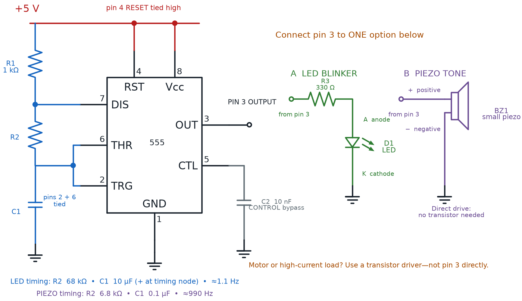
The 555 LED Blinker
A 555 LED Blinker is a 555 timer in astable mode wired so its output pin drives an LED through a current-limiting resistor, turning the chip's internal clock signal into something you can watch. Connect pin 3 to a 330 Ω resistor, then the LED's anode, then the LED's cathode back to ground — the exact same resistor-then-LED pattern from Chapter 12, just powered by a chip instead of a plain wire.
For a nice, easy-to-watch blink, Chapter 14's own table already did the math: R1 = 1 kΩ, R2 = 68 kΩ, and C = 10 µF gives a frequency of about 1.1 Hz — a little slower than once per second, plenty of time to see each on and off.
The 555 Buzzer Driver
A 555 Buzzer Driver is the same astable 555 circuit, but with a small piezo buzzer connected across pin 3 and ground instead of an LED. The 555's output can source enough current to drive a small buzzer directly — no transistor needed, unlike the motor from Chapter 13, which draws far more current than a buzzer ever does.
Since a blink you can hear needs to happen a lot faster than a blink you can see, this build borrows a different row from Chapter 14's frequency table: R1 = 1 kΩ, R2 = 6.8 kΩ, and C = 0.1 µF gives a frequency near 990 Hz — solidly in the range of an audible tone.
Here's the side-by-side comparison of both builds.
| Feature | 555 LED Blinker | 555 Buzzer Driver |
|---|---|---|
| Output component | LED + 330 Ω resistor | Small piezo buzzer |
| R1 / R2 / C | 1 kΩ / 68 kΩ / 10 µF | 1 kΩ / 6.8 kΩ / 0.1 µF |
| Approx. frequency | ≈ 1.1 Hz | ≈ 990 Hz |
| What you notice | A slow, visible blink | A steady audible tone |
| Pin 3 connects to | Resistor → LED anode → GND | Buzzer lead → GND |
The Math Already Did the Work
 Notice neither build required a single new calculation — both rows came straight out of Chapter 14's astable table. That's the entire point of learning a formula: once it's solved, you get to reuse the answer forever.
The bigger idea underneath both builds: a clock signal, the high-low pattern from Chapter 14, doesn't care what it's connected to. Wire it to an LED and you get a blinker. Wire it to a buzzer and you get a beeper. That same "it doesn't care what's listening" idea is about to power something a lot more impressive than one blinking light.
Meet the 74HC595: Controlling 8 LEDs From 3 Wires
Picture wiring eight separate LEDs to eight separate control wires, one at a time, just to make a simple light show. That's a lot of wiring — and it gets worse fast if a project ever needs sixteen or twenty-four LEDs instead of eight. The 74HC595 exists to solve exactly that problem, and the way it solves it is genuinely clever.
A shift register is a chip that receives data one single bit at a time, over just one wire, and then remembers a whole row of those bits at once, spreading them across separate output pins. The 74HC595 specifically does this with eight outputs, using only three control wires to load any pattern you want — light zero LEDs, light all eight, or light any pattern in between, all from the same three wires.
Think of it like a bucket brigade passing water buckets down a line, one bucket at a time, until every position in the line is holding a bucket. Each "bucket" here is a single bit — a 1 (light the LED) or a 0 (leave it dark) — and the line has eight positions.
The Shift Register Bit Order is the order in which bits enter the chip and march through it: each new bit pushes every bit already inside over by one position, and the very first bit sent in eventually travels furthest, arriving last at the far end of the register. Send four bits in a row — 1, 0, 1, 1 — and after four shifts, the register holds that exact sequence, in that exact order, spread across four of its eight positions.
Getting a bit into the register takes a clock pulse. A Manual Clock Pulse is a single pulse on the shift clock pin, triggered by hand — pressing a button once sends exactly one new bit marching into the register, letting you watch the bit order happen in slow motion instead of a blur. That's precisely how you'll first experiment with the chip: one button press, one bit, one chance to watch it move.
The 74HC595 actually uses two separate clock pins, and the difference matters. SRCLK is the shift clock — every pulse moves one new bit into a hidden internal stage and nudges everything else over. RCLK is a second, separate clock — the storage clock — and only its pulse actually copies that hidden stage out to the visible Q0-Q7 output pins, all at once. That two-step design means your LEDs never flicker through half-finished patterns while you're still shifting bits in; they jump straight from one clean pattern to the next.
Two more pins override the register entirely, and they do very different jobs.
The Shift Register Output Enable pin (OE′, active low) doesn't touch the stored data at all — pulling it low turns the Q0-Q7 outputs on so the LEDs can light, and pulling it high blanks every LED instantly while the register keeps holding whatever pattern it had, ready to reappear the moment OE′ goes low again. It's a mute button, not a delete button.
The Shift Register Reset Pin (SRCLR′, active low) is the delete button — pulling it low actually erases every bit in the register back to zero, the same way as unplugging and replugging power, except instant and without touching a single wire.
Mute Button vs. Delete Button
 It's an easy mix-up: Output Enable hides the LEDs without touching the data, while Reset erases the data itself. Toggle the wrong pin while debugging a shift register project and you'll either see nothing lit (data's fine, just hidden) or see everything go dark for a completely different reason (data's actually gone). Knowing which one you flipped saves a lot of confused troubleshooting.
Now for the full pin list — every one of the 74HC595's 16 pins, with the job it does.
| Pin | Name | Function |
|---|---|---|
| 1 | Q1 | Parallel output 1 |
| 2 | Q2 | Parallel output 2 |
| 3 | Q3 | Parallel output 3 |
| 4 | Q4 | Parallel output 4 |
| 5 | Q5 | Parallel output 5 |
| 6 | Q6 | Parallel output 6 |
| 7 | Q7 | Parallel output 7 |
| 8 | GND | Connects to ground |
| 9 | QH′ (SER OUT) | Serial data out — feeds the next chip's SER pin when daisy-chaining |
| 10 | SRCLR′ (RESET) | Clears every stored bit to 0 when pulled low |
| 11 | SRCLK | Shift clock — each pulse moves one new bit in from SER |
| 12 | RCLK | Storage clock — copies the shifted bits out to Q0-Q7 |
| 13 | OE′ (OUTPUT ENABLE) | Turns the Q0-Q7 outputs on when pulled low |
| 14 | SER (DATA IN) | Serial data input — the next bit to shift in |
| 15 | Q0 | Parallel output 0 |
| 16 | VCC | Connects to the positive supply |
Two Classic Demo Projects
With the pins named, two demo builds show off exactly why this chip is worth learning. Both use the same wiring — eight LEDs, each through its own current-limiting resistor, one per Q0-Q7 pin.
- The 74HC595 LED Bar Graph lights the eight LEDs as a simple bar, useful for showing a level — turn on Q0 alone for "low," then Q0 through Q3 for "medium," then all eight for "full." It's the same idea as a volume meter or a battery-level indicator.
- The Binary Counting Display treats those same eight LEDs as a single 8-bit binary number, where each LED represents one power of two. Shifting the right pattern in and reading the LEDs left to right shows any number from 0 to 255 written out in on/off lights instead of digits.
How Many Patterns Can 8 LEDs Show?
where:
- \( N \) is the number of unique on/off patterns possible
- \( n \) is the number of bits (LEDs) in the register
For all eight outputs, that's \( N = 2^8 = 256 \) different patterns — every possible combination of eight LEDs being on or off, all reachable through the same three control wires.
Daisy-Chaining for More Outputs
Eight LEDs is impressive from three wires — but what if a project needs sixteen, or twenty-four? Daisy-Chained Shift Registers are two or more 74HC595 chips wired so the first chip's QH′ pin (its serial output) feeds directly into the second chip's SER pin (its serial input), while both chips share the very same SRCLK and RCLK lines.
- The first chip's register fills up after 8 pulses, exactly as before
- The 9th pulse pushes the very first bit right out of the first chip's QH′ pin and into the second chip's SER pin
- Continue clocking, and bits keep marching from chip to chip, filling both registers in sequence
- One RCLK pulse still updates every LED on both chips at once, because RCLK is shared
The result: eight more LEDs for the price of one more chip, still controlled by the exact same three wires you started with. Chain a third chip on and you've got 24 outputs from three wires. That's the "whoa, that's efficient" moment this chip is famous for.
Three Wires, Practically Unlimited LEDs
 Take a second to really sit with that: three control wires, and it doesn't matter if you're driving 8 LEDs or 80 — daisy-chain enough 74HC595s and the wire count never grows. That's not a small trick. It's the same idea real engineers use to control huge LED displays, and you just learned it.
Explore the whole chip below — press the manual clock button to step bits in one at a time, flip Output Enable and Reset to see the difference, chain a second chip, and try the binary counting mode.
Diagram: 74HC595 Shift Register LED Bar Graph and Daisy-Chain Explorer
74HC595 Shift Register LED Bar Graph and Daisy-Chain Explorer
Type: microsim
sim-id: 74hc595-shift-register-led-bar-graph
Library: p5.js
Status: Specified
Purpose: Let students step data bits into a 74HC595 one clock pulse at a time, observe the shift-register bit order as it marches toward Q7, distinguish Output Enable from Reset, extend the register by daisy-chaining a second chip, watch a binary-counting demo mode, and swap the manual clock button for the 555 timer's own oscillating output.
Bloom Taxonomy: Apply (L3). Bloom Verb: demonstrate, apply, experiment.
Learning objective: Given a sequence of data bits and clock pulses, demonstrate how the 74HC595's shift register bit order fills its eight outputs one pulse at a time, distinguish the effect of the Output Enable and Reset pins, and compare manually-clocked stepping to an automatic 555-driven clock.
Reuse check: An embeddings search (find-similar-templates, mode=reuse) for "Title: 74HC595 Shift Register LED Bar Graph and Daisy Chain Explorer | Topic: 74HC595 shift register bit order, manual clock pulse, output enable pin, reset pin, daisy-chained shift registers, binary counting display, LED bar graph, 555-driven automatic clock | Subjects: Electronics, Beginning Electronics, Digital Electronics | Grade Level: Junior High | Learning Objectives: Given a data bit and clock pulses, demonstrate how bits shift through a 74HC595 register into eight LEDs, and compare manual clock pulses to an automatic 555-driven clock" returned a top match of "Shift Register MicroSim" (dmccreary/digital-electronics, WHAT score 0.6959, recommendation "template") — above the 0.60 threshold, but built as a schematic-style logic-analyzer view of a 74HC594 (a related but different chip, with a separate output-storage register variant) rather than this book's rendered-breadboard format. A parallel keyword grep of microsims-data.json for "shift register" and "74HC595" surfaced the same catalog entry plus its sibling "Shift Register" sim (dmccreary/clocks-and-watches, also 74HC594-based); neither lists an explicit grade level, so a manual sanity check against their junior-high-appropriate subject tags ("Shift Register", "Serial to Parallel") confirms topical fit even though the implementation style differs. Used as a Template: (https://dmccreary.github.io/digital-electronics/sims/shift-register/) for the clock/bit-shift interaction pattern only — the breadboard rendering, 74HC595-specific pin behavior, daisy-chaining, and 555-driven clock toggle are written fresh with the breadboard-sim-generator skill, extending this project's own docs/sims/flip-flop/ (an unrelated NAND-based SR latch, not breadboard-rendered, so not reusable here either) with the newer breadboard format instead.
Canvas layout: Rendered breadboard on the left with a 74HC595 straddling the center channel, eight LEDs (each with its own resistor) wired to Q0-Q7, a push button wired to SRCLK for the manual clock pulse, and a second 74HC595 that appears when daisy-chain mode is toggled on; right side panel holds a "Clock Pulse" button, a data-bit input (0/1 toggle), an "Output Enable" checkbox, a "Reset" button, a "Daisy-Chain 2nd Chip" toggle, a "Binary Counting Demo" toggle, a "555-Driven Clock" toggle, and an infobox.
Components/elements involved: A rendered breadboard; a new bbShiftRegister595 component (16-pin DIP body drawn straddling the center channel, with SER, SRCLK, RCLK, OE′, SRCLR′, GND, VCC, and Q0-Q7 pins in their real datasheet positions, and internal 8-bit state tracked by the sim's own JavaScript rather than the DC solver); eight bbLED components with bbResistor current-limiters on Q0-Q7; a bbButton wired to SRCLK; a second bbShiftRegister595 instance whose SER pin wires to the first chip's QH′ pin and whose SRCLK/RCLK wire to the same control lines, shown only in daisy-chain mode.
Required interactivity: - Clicking "Clock Pulse" shifts the currently selected data bit into the register (SRCLK pulse), visually animating the bit's position moving one step toward Q7, and the infobox reports the new register contents in binary - Toggling the data-bit input (0/1) before the next clock pulse changes what value is shifted in next - Unchecking "Output Enable" instantly blanks all LEDs without changing the infobox's reported register contents; re-checking it restores the display, demonstrating OE′ is a mute, not a delete - Clicking "Reset" clears the register to all zeros and the infobox explicitly notes the difference from Output Enable - Toggling "Daisy-Chain 2nd Chip" adds a second 74HC595 wired from the first chip's QH′ to the second chip's SER, and further clock pulses (9 and beyond) visibly move a bit from chip 1 into chip 2 - Toggling "Binary Counting Demo" auto-increments the 8-bit pattern once per second, displaying the running decimal value (0-255) next to the LED pattern - Toggling "555-Driven Clock" replaces the manual push button with a simulated 555 astable output (using the Chapter 14 LED-blinker frequency, ≈1.1 Hz) automatically pulsing SRCLK, with the infobox noting "The 555's clock signal is now stepping the shift register for you" - Button "Reset View" returns to single-chip mode, Output Enable on, register cleared, manual clocking, data bit 1
Default state: Single 74HC595, Output Enable checked, register cleared (all LEDs off), data bit set to 1, manual clock mode, infobox reads "Press Clock Pulse to shift a 1 into the register and watch it move."
Data Visibility Requirements: Stage 1: Show the current 8-bit register contents as both LED pattern and binary text Stage 2: On each clock pulse, show which single bit moved and from which position to which Stage 3: Show the decimal value of the register when Binary Counting Demo is active Stage 4: Show which clock source (manual button or 555-driven) is currently active
Instructional Rationale: An Apply-level "demonstrate/experiment" objective calls for direct manipulation of the register one pulse at a time so students build an accurate mental model of shift-register bit order before trusting an automatic mode; the 555-driven toggle deliberately reuses Chapter 14's own timing values so the callback is concrete, not just named.
Color scheme: Thin blue current-flow dots on the SRCLK and RCLK control wires, orange dots on each lit LED's supply path, a highlighted yellow outline tracking the bit currently in motion, green accent on the "555-Driven Clock" toggle when active — consistent with this book's other digital-signal diagrams.
Responsive behavior: Breadboard view and the control/infobox panel stack vertically on narrow screens; the scope panel is not used in this sim so no width-based hiding is needed; all toggles and buttons remain full-width and touch-friendly below 640 px.
Implementation: p5.js, built with the breadboard-sim-generator skill, extending this repository's breadboard-lib.js with a new bbShiftRegister595 component that models the 74HC595's internal 8-bit shift-and-latch behavior in JavaScript (not the DC steady-state solver, since shifting is a discrete-event process) while reusing bbLED, bbResistor, and bbButton for the visible circuit.
The 555-Driven Shift Register
Here's where the two threads of this chapter tie together. Instead of pressing a button to pulse SRCLK by hand, connect a 555 timer's pin 3 (OUTPUT) — the exact same astable clock signal from the LED Blinker earlier in this chapter — straight to SRCLK instead.
A 555-Driven Shift Register is a 74HC595 whose SRCLK pin is pulsed automatically by a 555 timer's astable output instead of a manual button, so the register keeps advancing on its own, forever, at whatever frequency the 555's resistors and capacitor were chosen to produce. Swap in the LED Blinker's slow 1.1 Hz timing and you get a hands-free "walking light" chaser across all eight LEDs. Swap in faster timing and the pattern races by too quickly to follow with your eyes — which is itself a fun way to demonstrate just how fast a clock signal can really run.
You Already Built the Clock
Nothing new to calculate here — the 555 LED Blinker from earlier in this chapter is the clock source. Disconnect its LED, wire pin 3 to SRCLK instead, and the shift register starts stepping itself. That's two projects becoming one bigger project, for free.
IC Handling Skills for Any Chip
Step back for a second. This chapter and the last one wired up two very different chips — an 8-pin 555 and a 16-pin 74HC595 — and every single time, the same handling habits applied: find pin 1, orient the notch, seat it evenly, wire it carefully. Those habits are worth naming on their own, because they'll apply to every chip this course (or any future project) ever asks you to handle.
Every chip in this course's kit ships in a DIP Package — short for Dual In-line Package — a rectangular block of black plastic with two straight rows of metal legs running down its long sides, exactly the shape Chapter 14 introduced with the 555. A DIP's IC Pin Count is simply how many of those legs it has: 8 for the 555, 16 for the 74HC595, and anywhere from 14 to 28 or more for other chips you might meet down the road. More pins generally means a chip that does more — more inputs, more outputs, more internal features packed into one part.
Every one of those pins sits at the exact same Standard IC Pin Spacing: 0.1 inch (2.54 mm) between the centers of neighboring pins. That number isn't a coincidence — it's the exact same spacing between holes on a solderless breadboard, which is precisely why a DIP chip plugs straight into a breadboard without any adapter at all.
Chapter 14 already taught you to find pin 1 using a chip's notch. Many chips, including many 74HC595s, add a second marker as well. A Pin 1 Dot Marker is a small round dot or dimple molded or printed into one corner of a chip's case, sitting directly above pin 1 — a second, independent confirmation of orientation that works even if a notch is hard to see under classroom lighting. When a notch and a dot are both present, they always agree; when you can only find one of the two, that's the one you trust.
Reading a Datasheet Like a Pro
Every chip's manufacturer publishes a datasheet, and every datasheet includes a diagram showing exactly what this chapter's 74HC595 table already listed in words. A Datasheet Pinout Diagram is a top-down drawing of a chip showing its outline, its notch or dot marking pin 1, and every pin's number and function labeled around the edges — the master reference for wiring any chip correctly, the same way the pin table earlier in this chapter served as the master reference for the 74HC595.
Reading one is a skill on its own: find the notch or dot first, confirm it matches pin 1's position, then count pins counter-clockwise exactly the way Chapter 14 taught, checking each number against its printed label as you go. Get comfortable with that habit now, on a chip whose pins you already know, and it'll transfer instantly to a chip you've never seen before.
Diagram: 74HC595 Datasheet Pinout Diagram Reader
74HC595 Datasheet Pinout Diagram Reader
Type: infographic
sim-id: 74hc595-datasheet-pinout-reader
Library: p5.js
Status: Specified
Purpose: Teach the general skill of reading any DIP chip's datasheet pinout diagram, using the 74HC595's own 16 pins as the worked example, and reinforce the Pin 1 Dot Marker as a second orientation check alongside the notch from Chapter 14.
Bloom Taxonomy: Remember (L1) / Understand (L2). Bloom Verb: identify, describe, locate.
Learning objective: Given a top-down datasheet-style pinout diagram of a 16-pin DIP chip with both a notch and a pin-1 dot, identify pin 1, count the remaining pins counter-clockwise, and locate each pin's printed function label.
Reuse check: An embeddings search (find-similar-templates, mode=reuse) for "Title: 74HC595 Datasheet Pinout Diagram Reader | Topic: DIP package IC pin numbering from pin 1 dot marker, standard IC pin spacing, reading a datasheet pinout diagram | Subjects: Electronics, Beginning Electronics | Grade Level: Junior High | Learning Objectives: Identify pin 1 of a 16-pin DIP chip from its dot marker and correctly read each pin's function from a datasheet pinout diagram" returned a top match of "Shift Register MicroSim" (dmccreary/digital-electronics, WHAT score 0.5169, recommendation "generate") — below the 0.60 template threshold, since that catalog entry is a working circuit simulation rather than a pinout-reading exercise. A keyword grep of microsims-data.json for "IC pinout" and "DIP package" found no direct matches; the closest keyword hit, "Pico Pinout Explorer" (dmccreary/learning-micropython, grade levels 5-12, "Students can identify the function of each pin... by name and number"), confirms strong topical and grade-level precedent for a click-to-reveal pinout exercise, but is Pico-board-specific with no DIP/notch/dot logic, so it is not reused. This is written as a new specification, modeled directly on this book's own Chapter 14 "ic-pin-numbering-notch-orientation" click-to-reveal infographic (same repository, same style), extended from an 8-pin chip to a 16-pin chip and from notch-only orientation to notch-plus-dot orientation.
Canvas layout: Main area shows a rendered 16-pin DIP chip with a semicircular notch at one end and a small pin-1 dot in the corner nearest pin 1, straddling a drawn breadboard center-channel outline for context; right side panel holds a "Rotate 180°" button and an infobox.
Components/elements involved: Chip body outline; notch marker; pin-1 dot marker; sixteen numbered, individually clickable pin pads that reveal their 74HC595 names (Q1-Q7, GND, QH′, SRCLR′, SRCLK, RCLK, OE′, SER, Q0, VCC) once clicked; a highlighted "Pin 1" indicator near the notch and dot; breadboard center-channel outline.
Required interactivity: - Clicking any pin pad opens an infobox showing that pin's number, its counting position relative to the notch, and its 74HC595 function name pulled from the same pin table shown earlier in this chapter - Clicking the "Rotate 180°" button spins the chip's orientation; when rotated, both the notch and the dot move to the opposite end together, and clicking any pin shows a warning infobox explaining which pins would land on the wrong breadboard columns - Hovering the notch or the dot, in either orientation, highlights both together and displays "Notch and dot always agree — either one marks Pin 1" - Button "Reset" returns the chip to its correct, un-rotated orientation
Default state: Chip correctly oriented with the notch and dot at the left end, no pin selected, infobox reads "Click a pin, the notch, or the dot to see how a datasheet pinout diagram works."
Data Visibility Requirements: Stage 1: Show the notch and dot positions together with the label "Pin 1 starts here" Stage 2: On pin click, show that pin's number and counting direction from pin 1 Stage 3: On pin click, show that pin's 74HC595 function name Stage 4: On rotate, show which pins would be misaligned with their intended breadboard columns
Instructional Rationale: A Remember/Understand "identify/locate" objective calls for the same simple click-to-reveal exploration Chapter 14 used for the 555, matching this reading level's guidance to avoid unnecessary animation; extending it to 16 pins and a second orientation marker (the dot) gives students practice generalizing a skill they already trust to a less familiar chip.
Color scheme: Blue chip outline matching the site's primary theme color, orange notch and dot highlight matching the accent color, red highlight overlay when rotated to show pin mismatch — consistent with Chapter 14's IC pin numbering diagram.
Responsive behavior: The chip view and control panel stack vertically on narrow screens; pin pads remain large enough to tap comfortably on mobile.
Implementation: Plain p5.js, not the breadboard-sim-generator — a click-to-reveal orientation diagram, matching the approach of Chapter 14's IC pin numbering sim rather than a wired, solved circuit.
Inserting, Straddling, and Removing a Chip Safely
Reading a pinout diagram only matters once the chip is actually seated correctly. Three physical skills make that happen every time.
The IC Insertion Technique is the safe way to seat any DIP chip: line up the notch or dot with the diagram first, check that no pins are visibly bent underneath the case, set the chip squarely over its holes, and press down with even pressure at both ends of the case — never in the middle, which can flex and crack the plastic — until every pin is fully seated.
The Breadboard IC Straddle is positioning a DIP chip so its two rows of pins sit on opposite sides of the breadboard's center channel, with each row landing in a separate set of connected rows. Straddle the chip off-center by even one row and half its pins land in the wrong net entirely, silently breaking the whole circuit without a single visible sign that anything's wrong.
An IC Socket is a small DIP-shaped holder that plugs into the breadboard first, so the actual chip plugs into the socket's sturdier spring contacts instead of the breadboard's holes directly. A socket protects a chip from the wear of repeated insertion and removal, and it means a suspected-bad chip during troubleshooting can be swapped in seconds without stressing any of its own pins.
Removing a chip needs just as much care as inserting one. The IC Removal Technique is lifting a chip straight up and evenly, using a dedicated chip-puller tool or two small flat screwdrivers alternating gentle pressure at each end — never yanking with fingers, which tends to bend pins or snap them off entirely.
| Situation | Do | Don't |
|---|---|---|
| Before inserting | Check every pin is straight | Force a chip with a visibly bent pin |
| Inserting | Press evenly at both ends | Push down in the middle of the case |
| Orienting | Confirm notch/dot matches the diagram | Guess based on which way "looks right" |
| Removing | Pry evenly from both ends, or use a chip puller | Pull with fingers by yanking one side |
| Reusing a chip a lot | Use an IC socket | Repeatedly re-seat directly in breadboard holes |
| Handling any CMOS chip | Touch a grounded metal object first | Slide it across carpet or synthetic fabric |
A Bent Pin Doesn't Fix Itself
Forcing a chip in with one bent pin can fold that pin flat under the case, where you can't see it — and now the chip looks seated but one connection is silently missing. Always run a finger lightly along each row of pins before inserting, and catch the bend before it hides.
If a pin does get bent, it's usually fixable. Bent IC Pin Repair is gently straightening a bent pin with needle-nose pliers, using small, controlled bends rather than one big correction, and checking the pin's alignment against the breadboard's hole spacing before trying to reinsert the chip. Rushing this step tends to snap a pin instead of straightening it — patience matters more than speed here.
One last risk applies to nearly every chip in this course's kit, and it's invisible until it's too late. Static Discharge Risk is the danger that ordinary static electricity built up on your body — from walking across carpet, or just moving around on a dry day — can discharge through a chip's pins and silently damage its internal circuitry the instant you touch it. CMOS chips like the 74HC595 are especially sensitive to this, more so than the 555.
Ground Yourself First
Before handling a 74HC595 or any other CMOS chip, touch a grounded metal object — a bare metal table leg, an unpainted radiator, or the metal case of a plugged-in computer — for a second or two. That simple habit drains away any static charge before it ever reaches the chip's pins.
A Lot of New Names, One Familiar Pattern
 Sixteen pins, two chip-handling tools, and a whole page of do's and don'ts — that's a lot to land at once. You don't need to memorize every pin name today. You need the pattern: check the notch or dot, straddle the channel, seat it evenly, ground yourself first. That pattern works on every chip you'll ever meet.
Chapter Summary: Key Takeaways
You paid off Chapter 14's promise, met a chip that controls eight LEDs from three wires, and picked up handling skills that work on any chip you'll ever wire:
- The 555 LED Blinker and 555 Buzzer Driver reuse the exact same astable 555 circuit from Chapter 14 — only the output component and the timing values change
- The 74HC595 shift register uses Shift Register Bit Order to march bits in one at a time via a Manual Clock Pulse, then reveals them on Q0-Q7 through separate Shift Register Output Enable and Shift Register Reset Pin controls
- Daisy-Chained Shift Registers extend those eight outputs to 16, 24, or more using the exact same three control wires
- The Binary Counting Display and 74HC595 LED Bar Graph are the chip's two classic demo projects, and a 555-Driven Shift Register replaces the manual button with an automatic clock from Chapter 14's own 555 circuit
- Every DIP chip shares a DIP Package, an IC Pin Count, and a Standard IC Pin Spacing of 0.1 inch — which is exactly why they fit a breadboard so well
- A Pin 1 Dot Marker backs up the notch from Chapter 14, and a Datasheet Pinout Diagram is the master reference for reading any chip's pins correctly
- Safe handling means the right IC Insertion Technique, a correct Breadboard IC Straddle, an IC Socket when a chip will be reseated often, a careful IC Removal Technique, Bent IC Pin Repair when needed, and always respecting Static Discharge Risk
Chapter 16 puts the breadboard back in your hands directly — wiring switches and buttons, and combining them into AND and OR logic without a single line of code or, this time, a single chip.
Shift Register Commander: Unlocked
 Huge chapter, builder! You blinked and beeped with the 555, then unlocked the superpower of controlling eight — or eighty — LEDs from just three wires. Add in safe handling for any chip you'll ever meet, and you're officially ready for whatever comes next. Current's flowing your way — see you in Chapter 16!